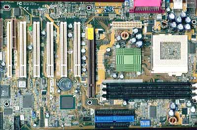
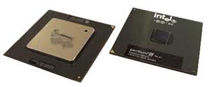
| Socket 370 |
|---|
| Intel Processors | Natural State | Sockets | L1/L2 Cache (Associativity) | Transistors |
|---|
Celeron-300A MMX
(Mendocino)
November 30, 1998 - ($70) | 370 pins
300MHz (66x4.5)
2.0v | Socket 370 | 16KB data (4-way)
16KB instruction (4-way)
128KB on-Die unified L2 (4-way)
* 4GB cacheable | 19 million
0.25&##181;m process
154mm&##178; die |
Celeron-333 MMX
(Mendocino)
November 30, 1998 - ($87) | 370 pins
333MHz (66x5.0)
2.0v | Socket 370 | 16KB data (4-way)
16KB instruction (4-way)
128KB on-Die unified L2 (4-way)
* 4GB cacheable | 19 million
0.25&##181;m process
154mm&##178; die |
Celeron-366 MMX
(Mendocino)
January 4, 1999 - ($123) | 370 pins
366MHz (66x5.5)
2.0v | Socket 370 | 16KB data (4-way)
16KB instruction (4-way)
128KB on-Die unified L2 (4-way)
* 4GB cacheable | 19 million
0.25&##181;m process
154mm&##178; die |
Celeron-400 MMX
(Mendocino)
January 4, 1999 - ($158) | 370 pins
400MHz (66x6.0)
2.0v | Socket 370 | 16KB data (4-way)
16KB instruction (4-way)
128KB on-Die unified L2 (4-way)
* 4GB cacheable | 19 million
0.25&##181;m process
154mm&##178; die |
Celeron-433 MMX
(Mendocino)
March 22, 1999 - ($169) | 370 pins
433MHz (66x6.5)
2.0v | Socket 370 | 16KB data (4-way)
16KB instruction (4-way)
128KB on-Die unified L2 (4-way)
* 4GB cacheable | 19 million
0.25&##181;m process
154mm&##178; die |
Celeron-466 MMX
(Mendocino)
April 26, 1999 - ($169) | 370 pins
466MHz (66x7.0)
2.0v | Socket 370 | 16KB data (4-way)
16KB instruction (4-way)
128KB on-Die unified L2 (4-way)
* 4GB cacheable | 19 million
0.25&##181;m process
154mm&##178; die |
Celeron-500 MMX
(Mendocino)
August 2, 1999 - ($167) | 370 pins
500MHz (66x7.5)
2.0v | Socket 370 | 16KB data (4-way)
16KB instruction (4-way)
128KB on-Die unified L2 (4-way)
* 4GB cacheable | 19 million
0.25&##181;m process
154mm&##178; die |
Celeron-533 MMX
(Mendocino)
January 4, 2000 - ($167) | 370 pins
533MHz (66x8.0)
2.0v | Socket 370 | 16KB data (4-way)
16KB instruction (4-way)
128KB on-Die unified L2 (4-way)
* 4GB cacheable | 19 million
0.25&##181;m process
154mm&##178; die |
Celeron-500A MMX SSE
(Coppermine-128)
March 29, 2000 (may not exist) | 370 pins
500MHz (66x7.5)
1.5v or 1.7v | Socket 370
(FC-PGA) | 16KB data (4-way)
16KB instruction (4-way)
128KB on-Die unified L2 (4-way)
* 4GB cacheable | 28 million
0.18&##181;m process
105mm&##178; die |
Celeron-533A MMX SSE
(Coppermine-128)
March 29, 2000 | 370 pins
533MHz (66x8.0)
1.5v or 1.7v | Socket 370
(FC-PGA) | 16KB data (4-way)
16KB instruction (4-way)
128KB on-Die unified L2 (4-way)
* 4GB cacheable | 28 million
0.18&##181;m process
105mm&##178; die
90mm&##178; die (Jun 00) |
Celeron-566 MMX SSE
(Coppermine-128)
March 29, 2000 - ($167) | 370 pins
566MHz (66x8.5)
1.5v or 1.7v | Socket 370
(FC-PGA) | 16KB data (4-way)
16KB instruction (4-way)
128KB on-Die unified L2 (4-way)
* 4GB cacheable | 28 million
0.18&##181;m process
105mm&##178; die
90mm&##178; die (Jun 00) |
Celeron-600 MMX SSE
(Coppermine-128)
March 29, 2000 - ($181) | 370 pins
600MHz (66x9.0)
1.5v or 1.7v or 1.75v | Socket 370
(FC-PGA) | 16KB data (4-way)
16KB instruction (4-way)
128KB on-Die unified L2 (4-way)
* 4GB cacheable | 28 million
0.18&##181;m process
105mm&##178; die
90mm&##178; die (Jun 00) |
Celeron-633 MMX SSE
(Coppermine-128)
June 26, 2000 - ($138) | 370 pins
633MHz (66x9.5)
1.65v or 1.7v or 1.75v | Socket 370
(FC-PGA) | 16KB data (4-way)
16KB instruction (4-way)
128KB on-Die unified L2 (4-way)
* 4GB cacheable | 28 million
0.18&##181;m process
105mm&##178; die
90mm&##178; die (Jun 00) |
Celeron-667 MMX SSE
(Coppermine-128)
June 26, 2000 - ($170) | 370 pins
666MHz (66x10.0)
1.65v or 1.7v or 1.75v | Socket 370
(FC-PGA) | 16KB data (4-way)
16KB instruction (4-way)
128KB on-Die unified L2 (4-way)
* 4GB cacheable | 28 million
0.18&##181;m process
105mm&##178; die
90mm&##178; die (Jun 00) |
Celeron-700 MMX SSE
(Coppermine-128)
June 26, 2000 - ($192) | 370 pins
700MHz (66x10.5)
1.65v or 1.7v or 1.75v | Socket 370
(FC-PGA) | 16KB data (4-way)
16KB instruction (4-way)
128KB on-Die unified L2 (4-way)
* 4GB cacheable | 28 million
0.18&##181;m process
105mm&##178; die
90mm&##178; die (Jun 00) |
Celeron-733 MMX SSE
(Coppermine-128)
November 13, 2000 - ($112) | 370 pins
733MHz (66x11.0)
1.65v or 1.7v | Socket 370
(FC-PGA) | 16KB data (4-way)
16KB instruction (4-way)
128KB on-Die unified L2 (4-way)
* 4GB cacheable | 28 million
0.18&##181;m process
90mm&##178; die
95mm&##178; die (Jul 01) |
Celeron-766 MMX SSE
(Coppermine-128)
November 13, 2000 - ($170) | 370 pins
766MHz (66x11.5)
1.65v or 1.7v | Socket 370
(FC-PGA) | 16KB data (4-way)
16KB instruction (4-way)
128KB on-Die unified L2 (4-way)
* 4GB cacheable | 28 million
0.18&##181;m process
90mm&##178; die |
Celeron-800 MMX SSE
(Coppermine-128)
January 3, 2001 - ($170) | 370 pins
800MHz (100x8.0)
1.65v or 1.7v or 1.75v | Socket 370
(FC-PGA) | 16KB data (4-way)
16KB instruction (4-way)
128KB on-Die unified L2 (4-way)
* 4GB cacheable | 28 million
0.18&##181;m process
90mm&##178; die
95mm&##178; die (Jul 01) |
Celeron-850 MMX SSE
(Coppermine-128)
April 9, 2001 - ($138) | 370 pins
850MHz (100x8.5)
1.65v or 1.7v or 1.75v | Socket 370
(FC-PGA) | 16KB data (4-way)
16KB instruction (4-way)
128KB on-Die unified L2 (4-way)
* 4GB cacheable | 28 million
0.18&##181;m process
90mm&##178; die
95mm&##178; die (Jul 01) |
Celeron-900 MMX SSE
(Coppermine-128)
July 2, 2001 - ($103) | 370 pins
900MHz (100x9.0)
1.75v | Socket 370
(FC-PGA)
(FC-PGA2) | 16KB data (4-way)
16KB instruction (4-way)
128KB on-Die unified L2 (4-way)
* 4GB cacheable | 28 million
0.18&##181;m process
95mm&##178; die |
Celeron-950 MMX SSE
(Coppermine-128)
August 31, 2001 - ($74) | 370 pins
950MHz (100x9.5)
1.75v | Socket 370
(FC-PGA)
(FC-PGA2) | 16KB data (4-way)
16KB instruction (4-way)
128KB on-Die unified L2 (4-way)
* 4GB cacheable | 28 million
0.18&##181;m process
95mm&##178; die |
Celeron-1.0G MMX SSE
(Coppermine-128)
August 31, 2001 - ($89) | 370 pins
1000MHz (100x10.0)
1.75v | Socket 370
(FC-PGA)
(FC-PGA2) | 16KB data (4-way)
16KB instruction (4-way)
128KB on-Die unified L2 (4-way)
* 4GB cacheable | 28 million
0.18&##181;m process
95mm&##178; die |
Celeron-1.1G MMX SSE
(Coppermine-128)
August 31, 2001 - ($103) | 370 pins
1100MHz (100x11.0)
1.75v | Socket 370
(FC-PGA)
(FC-PGA2) | 16KB data (4-way)
16KB instruction (4-way)
128KB on-Die unified L2 (4-way)
* 4GB cacheable | 28 million
0.18&##181;m process
95mm&##178; die |
Celeron-1.0A MMX SSE
(Tualatin)
January 3, 2002 | 370 pins
1000MHz (100x10.0)
1.475v | Socket 370
(FC-PGA2)
1.25v AGTL | 16KB data (4-way)
16KB instruction (4-way)
256KB on-Die unified L2 (8-way)
* 4GB cacheable | 44 million
0.13&##181;m process
80mm&##178; die |
Celeron-1.1A MMX SSE
(Tualatin)
January 3, 2002 | 370 pins
1100MHz (100x11.0)
1.475v | Socket 370
(FC-PGA2)
1.25v AGTL | 16KB data (4-way)
16KB instruction (4-way)
256KB on-Die unified L2 (8-way)
* 4GB cacheable | 44 million
0.13&##181;m process
80mm&##178; die |
Celeron-1.2G MMX SSE
(Tualatin)
October 2, 2001 - ($103) | 370 pins
1200MHz (100x12.0)
1.475v or 1.5v | Socket 370
(FC-PGA2)
1.25v AGTL | 16KB data (4-way)
16KB instruction (4-way)
256KB on-Die unified L2 (8-way)
* 4GB cacheable | 44 million
0.13&##181;m process
80mm&##178; die |
Celeron-1.3G MMX SSE
(Tualatin)
January 3, 2002 - ($118) | 370 pins
1300MHz (100x13.0)
1.5v | Socket 370
(FC-PGA2)
1.25v AGTL | 16KB data (4-way)
16KB instruction (4-way)
256KB on-Die unified L2 (8-way)
* 4GB cacheable | 44 million
0.13&##181;m process
80mm&##178; die |
Celeron-1.4G MMX SSE
(Tualatin)
2Q 2002? | 370 pins
1400MHz (100x14.0)
?v | Socket 370
(FC-PGA2)
1.25v AGTL | 16KB data (4-way)
16KB instruction (4-way)
256KB on-Die unified L2 (8-way)
* 4GB cacheable | 44 million
0.13&##181;m process
80mm&##178; die |
Celeron-1.5G MMX SSE
(Tualatin)
3Q 2002? | 370 pins
1500MHz (100x15.0)
?v | Socket 370
(FC-PGA2)
1.25v AGTL | 16KB data (4-way)
16KB instruction (4-way)
256KB on-Die unified L2 (8-way)
* 4GB cacheable | 44 million
0.13&##181;m process
80mm&##178; die |
Pentium III-500E MMX SSE
(Coppermine)
October 25, 1999 - ($239) | 370 pins
500MHz (100x5.0)
1.6v | Socket 370
(FC-PGA) | 16KB data (4-way)
16KB instruction (4-way)
256KB on-Die unified L2 (8-way)
* 4GB cacheable | 28 million
0.18&##181;m process
106mm&##178; die
105mm&##178; die (Mar 00) |
Pentium III-533EB MMX SSE
(Coppermine)
March 1, 2000 | 370 pins
533MHz (133x4.0)
1.65v | Socket 370
(FC-PGA) | 16KB data (4-way)
16KB instruction (4-way)
256KB on-Die unified L2 (8-way)
* 4GB cacheable | 28 million
0.18&##181;m process
106mm&##178; die
105mm&##178; die (Mar 00) |
Pentium III-550E MMX SSE
(Coppermine)
October 25, 1999 - ($368) | 370 pins
550MHz (100x5.5)
1.6v or 1.65v or 1.7v | Socket 370
(FC-PGA) | 16KB data (4-way)
16KB instruction (4-way)
256KB on-Die unified L2 (8-way)
* 4GB cacheable | 28 million
0.18&##181;m process
106mm&##178; die
105mm&##178; die (Mar 00)
90mm&##178; die (Jul 00) |
Pentium III-600E MMX SSE
(Coppermine)
March 1, 2000 | 370 pins
600MHz (100x6.0)
1.65v or 1.7v | Socket 370
(FC-PGA) | 16KB data (4-way)
16KB instruction (4-way)
256KB on-Die unified L2 (8-way)
* 4GB cacheable | 28 million
0.18&##181;m process
106mm&##178; die
105mm&##178; die (Mar 00)
90mm&##178; die (Jul 00)
95mm&##178; die (May 01) |
Pentium III-600EB MMX SSE
(Coppermine)
March 1, 2000 | 370 pins
600MHz (133x4.5)
1.65v or 1.7v | Socket 370
(FC-PGA) | 16KB data (4-way)
16KB instruction (4-way)
256KB on-Die unified L2 (8-way)
* 4GB cacheable | 28 million
0.18&##181;m process
106mm&##178; die
105mm&##178; die (Mar 00)
90mm&##178; die (Jul 00) |
Pentium III-650 MMX SSE
(Coppermine)
March 1, 2000 | 370 pins
650MHz (100x6.5)
1.65v or 1.7v | Socket 370
(FC-PGA) | 16KB data (4-way)
16KB instruction (4-way)
256KB on-Die unified L2 (8-way)
* 4GB cacheable | 28 million
0.18&##181;m process
106mm&##178; die
105mm&##178; die (Mar 00)
90mm&##178; die (Jul 00) |
Pentium III-667 MMX SSE
(Coppermine)
March 1, 2000 | 370 pins
666MHz (133x5.0)
1.65v or 1.7v | Socket 370
(FC-PGA) | 16KB data (4-way)
16KB instruction (4-way)
256KB on-Die unified L2 (8-way)
* 4GB cacheable | 28 million
0.18&##181;m process
106mm&##178; die
105mm&##178; die (Mar 00)
90mm&##178; die (Jul 00) |
Pentium III-700 MMX SSE
(Coppermine)
March 1, 2000 | 370 pins
700MHz (100x7.0)
1.65v or 1.7v or 1.75v | Socket 370
(FC-PGA) | 16KB data (4-way)
16KB instruction (4-way)
256KB on-Die unified L2 (8-way)
* 4GB cacheable | 28 million
0.18&##181;m process
106mm&##178; die
105mm&##178; die (Mar 00)
90mm&##178; die (Jul 00)
95mm&##178; die (May 01) |
Pentium III-733 MMX SSE
(Coppermine)
March 1, 2000 | 370 pins
733MHz (133x5.5)
1.65v or 1.7v or 1.75v | Socket 370
(FC-PGA) | 16KB data (4-way)
16KB instruction (4-way)
256KB on-Die unified L2 (8-way)
* 4GB cacheable | 28 million
0.18&##181;m process
106mm&##178; die
105mm&##178; die (Mar 00)
90mm&##178; die (Jul 00) |
Pentium III-750 MMX SSE
(Coppermine)
March 1, 2000 | 370 pins
750MHz (100x7.5)
1.65v or 1.7v or 1.75v | Socket 370
(FC-PGA) | 16KB data (4-way)
16KB instruction (4-way)
256KB on-Die unified L2 (8-way)
* 4GB cacheable | 28 million
0.18&##181;m process
106mm&##178; die
105mm&##178; die (Mar 00)
90mm&##178; die (Jul 00)
95mm&##178; die (May 01) |
Pentium III-800E MMX SSE
(Coppermine)
March 1, 2000 | 370 pins
800MHz (100x8.0)
1.65v or 1.7v or 1.75v | Socket 370
(FC-PGA) | 16KB data (4-way)
16KB instruction (4-way)
256KB on-Die unified L2 (8-way)
* 4GB cacheable | 28 million
0.18&##181;m process
106mm&##178; die
105mm&##178; die (Mar 00)
90mm&##178; die (Jul 00) |
Pentium III-800EB MMX SSE
(Coppermine)
March 1, 2000 | 370 pins
800MHz (133x6.0)
1.65v or 1.7v or 1.75v | Socket 370
(FC-PGA) | 16KB data (4-way)
16KB instruction (4-way)
256KB on-Die unified L2 (8-way)
* 4GB cacheable | 28 million
0.18&##181;m process
106mm&##178; die
105mm&##178; die (Mar 00)
90mm&##178; die (Jul 00)
95mm&##178; die (May 01) |
Pentium III-850 MMX SSE
(Coppermine)
March 20, 2000 - ($765) | 370 pins
850MHz (100x8.5)
1.65v or 1.7v or 1.75v | Socket 370
(FC-PGA) | 16KB data (4-way)
16KB instruction (4-way)
256KB on-Die unified L2 (8-way)
* 4GB cacheable | 28 million
0.18&##181;m process
105mm&##178; die
90mm&##178; die (Jul 00) |
Pentium III-866 MMX SSE
(Coppermine)
March 20, 2000 - ($776) | 370 pins
866MHz (133x6.5)
1.65v or 1.7v or 1.75v | Socket 370
(FC-PGA) | 16KB data (4-way)
16KB instruction (4-way)
256KB on-Die unified L2 (8-way)
* 4GB cacheable | 28 million
0.18&##181;m process
105mm&##178; die
90mm&##178; die (Jul 00)
95mm&##178; die (May 01) |
Pentium III-900 MMX SSE
(Coppermine)
October, 2000 | 370 pins
900MHz (100x9.0)
1.7v | Socket 370
(FC-PGA) | 16KB data (4-way)
16KB instruction (4-way)
256KB on-Die unified L2 (8-way)
* 4GB cacheable | 28 million
0.18&##181;m process
90mm&##178; die
95mm&##178; die (May 01) |
Pentium III-933 MMX SSE
(Coppermine)
May 24, 2000 - ($744) | 370 pins
933MHz (133x7.0)
1.65v or 1.7v or 1.75v | Socket 370
(FC-PGA) | 16KB data (4-way)
16KB instruction (4-way)
256KB on-Die unified L2 (8-way)
* 4GB cacheable | 28 million
0.18&##181;m process
105mm&##178; die
90mm&##178; die (Jul 00)
95mm&##178; die (May 01) |
Pentium III-1.0G MMX SSE
(Coppermine)
June, 2001 | 370 pins
1000MHz (100x10.0)
1.75v | Socket 370
(FC-PGA) | 16KB data (4-way)
16KB instruction (4-way)
256KB on-Die unified L2 (8-way)
* 4GB cacheable | 28 million
0.18&##181;m process
95mm&##178; die |
Pentium III-1.0B MMX SSE
(Coppermine)
January, 2001 | 370 pins
1000MHz (133x7.5)
1.7v or 1.75v or 1.76v | Socket 370
(FC-PGA)
(FC-PGA2) | 16KB data (4-way)
16KB instruction (4-way)
256KB on-Die unified L2 (8-way)
* 4GB cacheable | 28 million
0.18&##181;m process
90mm&##178; die
95mm&##178; die (May 01) |
Pentium III-1.1G MMX SSE
(Coppermine)
June, 2001 | 370 pins
1100MHz (100x11.0)
1.75v | Socket 370
(FC-PGA) | 16KB data (4-way)
16KB instruction (4-way)
256KB on-Die unified L2 (8-way)
* 4GB cacheable | 28 million
0.18&##181;m process
95mm&##178; die |
Pentium III-1.13G MMX SSE
(Coppermine)
June, 2001 | 370 pins
1133MHz (133x8.5)
1.75v | Socket 370
(FC-PGA) | 16KB data (4-way)
16KB instruction (4-way)
256KB on-Die unified L2 (8-way)
* 4GB cacheable | 28 million
0.18&##181;m process
95mm&##178; die |
Pentium III-866 MMX SSE
(Coppermine-T)
June, 2001 | 370 pins
866MHz (133x6.5)
1.75v | Socket 370
(FC-PGA)
1.5v AGTL+
1.25v AGTL | 16KB data (4-way)
16KB instruction (4-way)
256KB on-Die unified L2 (8-way)
* 4GB cacheable | 28 million
0.18&##181;m process
95mm&##178; die |
Pentium III-933 MMX SSE
(Coppermine-T)
June, 2001 | 370 pins
933MHz (133x7.0)
1.75v | Socket 370
(FC-PGA)
1.5v AGTL+
1.25v AGTL | 16KB data (4-way)
16KB instruction (4-way)
256KB on-Die unified L2 (8-way)
* 4GB cacheable | 28 million
0.18&##181;m process
95mm&##178; die |
Pentium III-1.0B MMX SSE
(Coppermine-T)
June, 2001 | 370 pins
1000MHz (133x7.5)
1.75v | Socket 370
(FC-PGA2)
1.5v AGTL+
1.25v AGTL | 16KB data (4-way)
16KB instruction (4-way)
256KB on-Die unified L2 (8-way)
* 4GB cacheable | 28 million
0.18&##181;m process
95mm&##178; die |
Pentium III-1.13G MMX SSE
(Coppermine-T)
June, 2001 | 370 pins
1133MHz (133x8.5)
1.75v | Socket 370
(FC-PGA2)
1.5v AGTL+
1.25v AGTL | 16KB data (4-way)
16KB instruction (4-way)
256KB on-Die unified L2 (8-way)
* 4GB cacheable | 28 million
0.18&##181;m process
95mm&##178; die |
Pentium III-1.13A MMX SSE
(Tualatin)
July, 2001 | 370 pins
1133MHz (133x8.5)
1.475v | Socket 370
(FC-PGA2)
1.25v AGTL | 16KB data (4-way)
16KB instruction (4-way)
256KB on-Die unified L2 (8-way)
* 64GB cacheable | 44 million
0.13&##181;m process
80mm&##178; die |
Pentium III-1.2G MMX SSE
(Tualatin)
July, 2001 | 370 pins
1200MHz (133x9.0)
1.475v | Socket 370
(FC-PGA2)
1.25v AGTL | 16KB data (4-way)
16KB instruction (4-way)
256KB on-Die unified L2 (8-way)
* 64GB cacheable | 44 million
0.13&##181;m process
80mm&##178; die |
Pentium III-S-700 MMX SSE
(Tualatin)
November 13, 2001 | 370 pins
700MHz (100x7.0)
1.1v | Socket 370
(FC-PGA2)
1.25v AGTL | 16KB data (4-way)
16KB instruction (4-way)
512KB on-Die unified L2 (8-way)
* 64GB cacheable | 44 million
0.13&##181;m process
80mm&##178; die |
Pentium III-S-800 MMX SSE
(Tualatin)
1Q 2002? | 370 pins
800MHz (133x6.0)
?v or 1.1v | Socket 370
(FC-PGA2)
1.25v AGTL | 16KB data (4-way)
16KB instruction (4-way)
512KB on-Die unified L2 (8-way)
* 64GB cacheable | 44 million
0.13&##181;m process
80mm&##178; die |
Pentium III-S-900 MMX SSE
(Tualatin)
3Q 2002? | 370 pins
900MHz (100x9.0)
?v | Socket 370
(FC-PGA2)
1.25v AGTL | 16KB data (4-way)
16KB instruction (4-way)
512KB on-Die unified L2 (8-way)
* 64GB cacheable | 44 million
0.13&##181;m process
80mm&##178; die |
Pentium III-S-933 MMX SSE
(Tualatin)
3Q 2002? | 370 pins
933MHz (133x7.0)
1.1v | Socket 370
(FC-PGA2)
1.25v AGTL | 16KB data (4-way)
16KB instruction (4-way)
512KB on-Die unified L2 (8-way)
* 64GB cacheable | 44 million
0.13&##181;m process
8mm&##178; die |
Pentium III-S-1.0B MMX SSE
(Tualatin)
July 18, 2001 | 370 pins
1000MHz (133x7.5)
1.45v | Socket 370
(FC-PGA2)
1.25v AGTL | 16KB data (4-way)
16KB instruction (4-way)
256KB on-Die unified L2 (8-way)
* 64GB cacheable | 44 million
0.13&##181;m process
80mm&##178; die |
Pentium III-S-1.13G MMX SSE
(Tualatin)
June 21, 2001 | 370 pins
1133MHz (133x8.5)
1.45v | Socket 370
(FC-PGA2)
1.25v AGTL | 16KB data (4-way)
16KB instruction (4-way)
512KB on-Die unified L2 (8-way)
* 64GB cacheable | 44 million
0.13&##181;m process
80mm&##178; die |
Pentium III-S-1.26G MMX SSE
(Tualatin)
July 18, 2001 | 370 pins
1266MHz (133x9.5)
1.45v | Socket 370
(FC-PGA2)
1.25v AGTL | 16KB data (4-way)
16KB instruction (4-way)
512KB on-Die unified L2 (8-way)
* 64GB cacheable | 44 million
0.13&##181;m process
80mm&##178; die |
Pentium III-S-1.4G MMX SSE
(Tualatin)
January 8, 2002 - ($315) | 370 pins
1400MHz (133x10.5)
1.45v | Socket 370
(FC-PGA2)
1.25v AGTL | 16KB data (4-way)
16KB instruction (4-way)
512KB on-Die unified L2 (8-way)
* 64GB cacheable | 44 million
0.13&##181;m process
80mm&##178; die |
Pentium III-S-1.53G MMX SSE
(Tualatin)
3Q 2002? | 370 pins
1533MHz (133x11.5)
1.45v | Socket 370
(FC-PGA2)
1.25v AGTL | 16KB data (4-way)
16KB instruction (4-way)
512KB on-Die unified L2 (8-way)
* 64GB cacheable | 44 million
0.13&##181;m process
80mm&##178; die |
COMMENTS FOR:
'PC - M'board Socket - (P3/Celeron)'
There are a total: 1 comments posted to this page.
Last added comment
Article 'ratings' were added September 2008, so most articles have no viewer rating
[back to top]